FPGAs at the Quantum Matter Institute
<< click to return to front page
<< click to return to content page
This post has a little longer outline than usual. If you want to skip to just the FPGA content, scroll down to the table of contents.
- RTL Design and DSP Simulation (Verilog in Vivado, MATLAB)
- Server-Client Networking (C, Python)
- Control Theory, Signal Processing, Circuit Design
- Measurements and Data Collection (SR780)
This page highlights some of the interesting work and things I’ve designed for my project with Stewart Blusson Quantum Matter Institute (SBQMI, or QMI) at UBC. In short, I am developing FPGA control loop applications entirely from scratch to lock a femtosecond enhancement cavity. Along the way I’ve had the chance to dip into areas of signal processing, control theory, circuit design, server-client networking, and more!
Here’s some brief context helping to introduce the project better. Of course you can simply minimize this section and skip right to the takeaway (pink) and the actual work that follows.
Context
ARPES:
Angle-resolved photoemission spectroscopy refers to the technique of characterizing a sample’s surface on a nanometer scale, revealing atomic properties of the material.
To do so, a highly focused photon source is pointed at the sample. By the photo-electric effect, electrons are knocked off the surface of the sample.
The energy, momentum, and ejection angle of these electrons are measured in an electron spectrometer, helping researchers study the band structures of such samples.
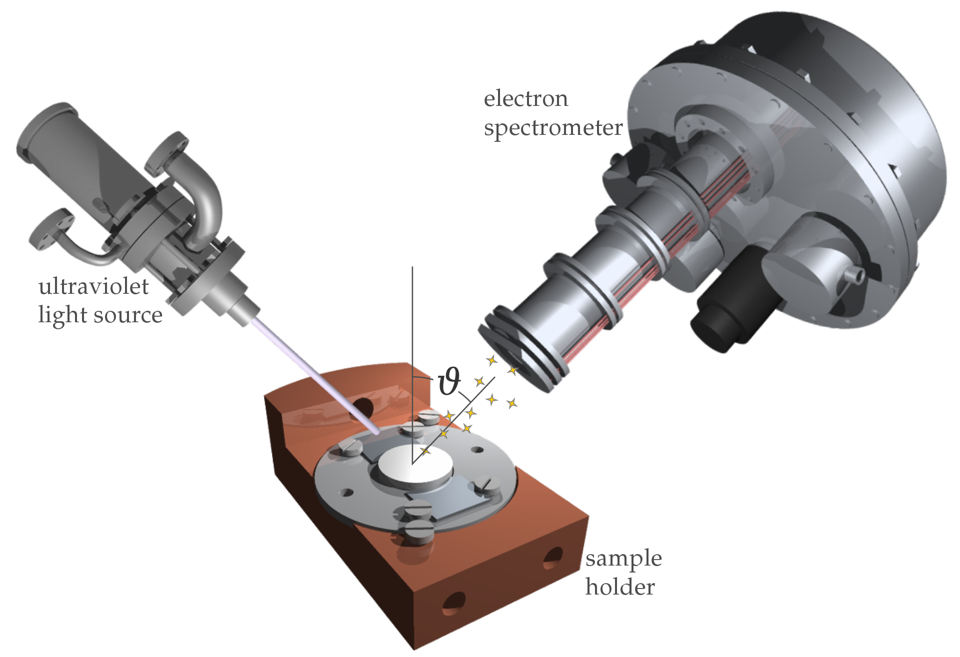
Photo 1 (top left) in the Project Photos section is the tr-ARPES setup from the outside.
XUV:
The first step in this ARPES process then is to derive some photon source, which provides the ionization energy to knock electrons off the sample.; our lab uses an XUV (extreme ultra-violet) source. XUV pulses are generated by HHG, which involves using a strong laser pulse to hit gas particles, which emit XUV light.
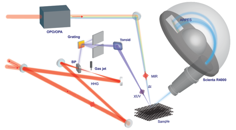
Unfortunately the type of laser you require to generate high power XUV pulses by HHG are not available, so we must use something called an enhancement cavity.
Enhancement Cavities:
An enhancement cavity builds up high-power lasers pulses from an incident, lower-intensity laser. In our spectroscopy scheme, it sits between the a low power laser source, and before HHG. This cavity is shown by the red beams above (they make a bow-tie shape). It’s also drawn here:
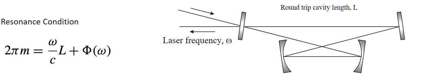
Simply put, if a laser pulse completes a round trip within the cavity exactly when a new incident laser pulse enters the cavity, they will constructively interfere and now the light in the cavity has increased. This is the “resonance condition”, and we often say that the laser is locked in this state.
Introducing the Project:
The simplest way to satisfy the resonance condition is to change the length of the cavity by changing the spacing of the mirrors. Simply do this until a resonance is reached, right? So, can’t we just perform some calculations, find the required cavity spacing, and then glue all the mirrors in place once we observe increased light building up?
Well, of course not, or I wouldn’t be writing this! Since the spacing of the mirrors must be adjusted on a nm level, external effects such as vibrations of the building, thermal expansion of the mirrors, and even speaking beside the laser table cause the system to fall out of resonance (called losing lock).
Instead what we do is place our mirrors on linear PZT actuators, and put together some system to dynamically change the mirror spacing as required.
Takeaway: We need a way to dynamically adjust the spacing of the mirrors (i.e. the length of the cavity) to hold onto the resonance, even under perturbations.
This sounds like a job for control loops … unless you wanted to describe how virtually indetectable vibrations of a building, varying temperatures, and sound waves travelling the room would affect the system.
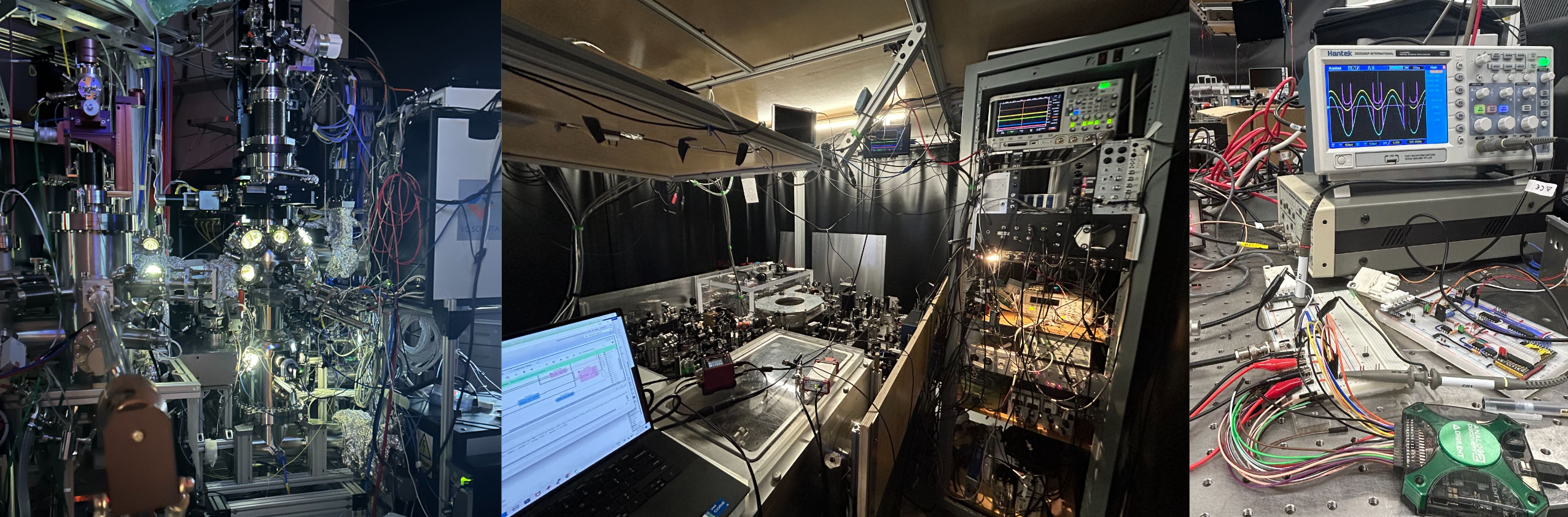
Okay, so we’re using a control loop to change the length of the cavity to hold onto a resonance. Every control loop needs an error signal, and in this case we use the Pound-Drever-Hall technique to generate one (shown below), to understand if we decrease or increase the length of the cavity to hold onto the resonance. Most commonly these control loops are done with analog circuits. Layers of integrators, multipliers, adders, and filters come together with mixers and phase shifters to create a traditional laser locking system. Speaking of such a system, here’s the one at QMI:
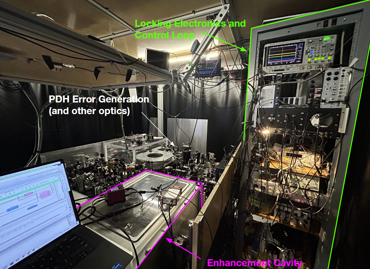
- On the left side is the laser table which, among many other things, generates the PDH error signal. It’s populated with mirrors, lenses, filters, and more, giving it the appearance of a skyscraper-filled city.
- Boxed in pink is the enhancement cavity itself, where the laser light accumulates and builds up power.
- Finally, and most importantly, are the locking electronics and control loop tower boxed in green, which puts everything all together. It takes in the PDH error signal and outputs signals which adjust the spacing of the enhancement cavity mirrors. In between lie all the analog integrators, mixers, and modulators I described earlier.
The focus of my work is to digitize as much of the analog locking electronics and control loop subsystems onto an FPGA
There are many reasons as to why an FPGA control loop would be preferred over an analog one, such as … - much easier to modify, upgrade, maintain, and troubleshoot - precisely tune loop parameters (gains, thresholds, offsets) rather than using knobs / switches - remotely monitor and work with the cavity, rather than being required to be present at all times
… alongside many other nice-to-haves, like reduced space.
The idea of FPGAs being used for locking cavities is not new. However, since everything about this project was built from scratch, my supervisor and I were able to learn a lot about using these devices, and also their pitfalls in comparison to analog locking electronics, which is somewhat undiscussed in other existing packages.
The rest of this page will serve as an image gallery with brief explanations, providing little snapshots into what I’ve explored.
- FPGA Block Designs
- Server-Client Networking
- FIR and CIC Filters
- PID Motor Control
1. FPGA Block Designs
This project is built entirely from scratch, using Verilog (in Vivado). The Red Pitaya board we use in this project has a whole library of user-built applications, and can also be programmed using MATLAB, Python, LabVIEW, and more. While these are simpler to work with, I found it more valuable to work from scratch — we were able to push our system as hard as we needed it, and even exceeded limits advertised by Red Pitaya with writing custom RTL.
Learning about TCL scripting → synthesis → implementation → timing analysis → bitstream generation has taught me about design rules and principles when working with FPGAs, and now I feel more comfortable using newer, more advanced hardware design languages.
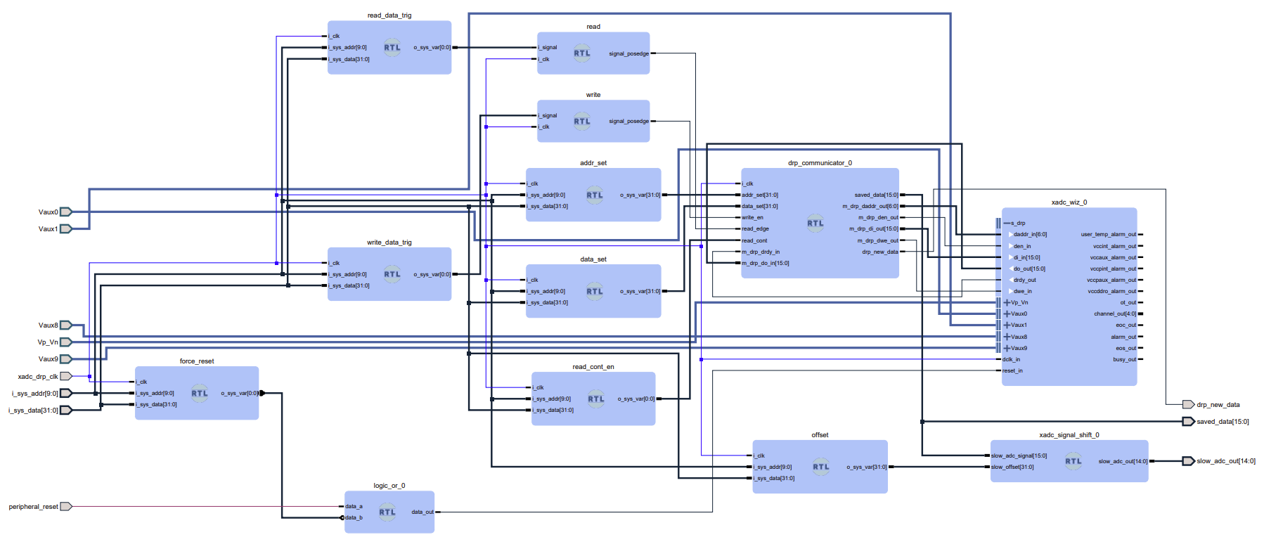
XADC:
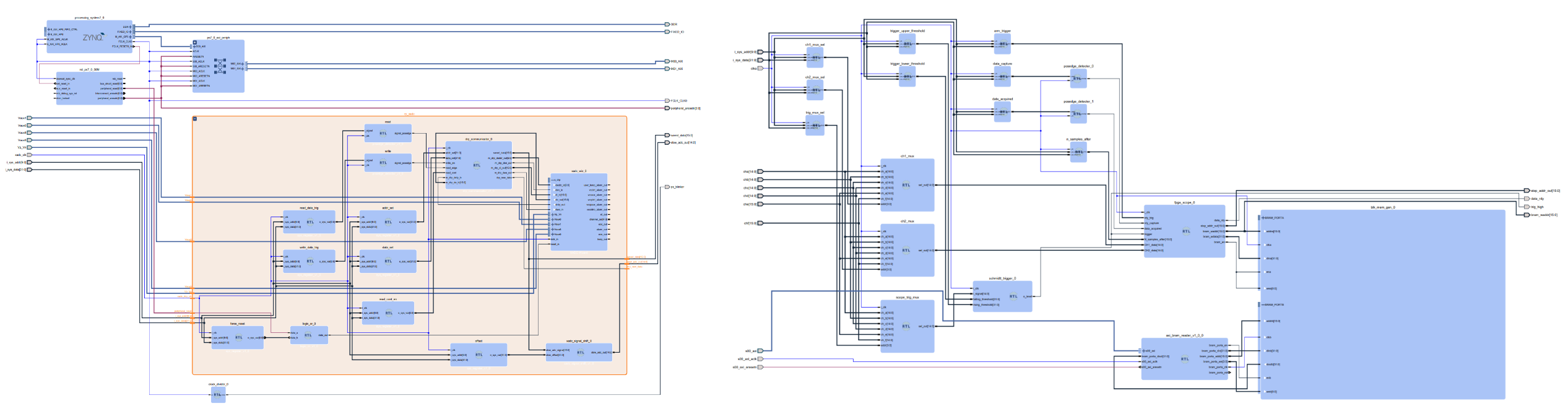
Here’s the block design of our processing system and XADC core, which interfaces with the Zynq 7010’s internal slower ADC running at 1 MSP/s…
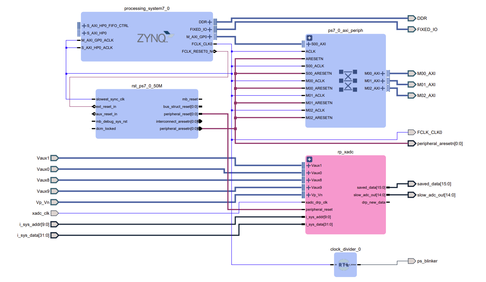
… expanding the rp_xadc module (pink) reveals the xadc_wiz.v and the associated drp_communicator.v. Our communicator module uses the DRP (dynamic reconfiguration port) on the XADC which allows us to calibrate, configure channels, and read data from internal hardware registers which store ADC data.
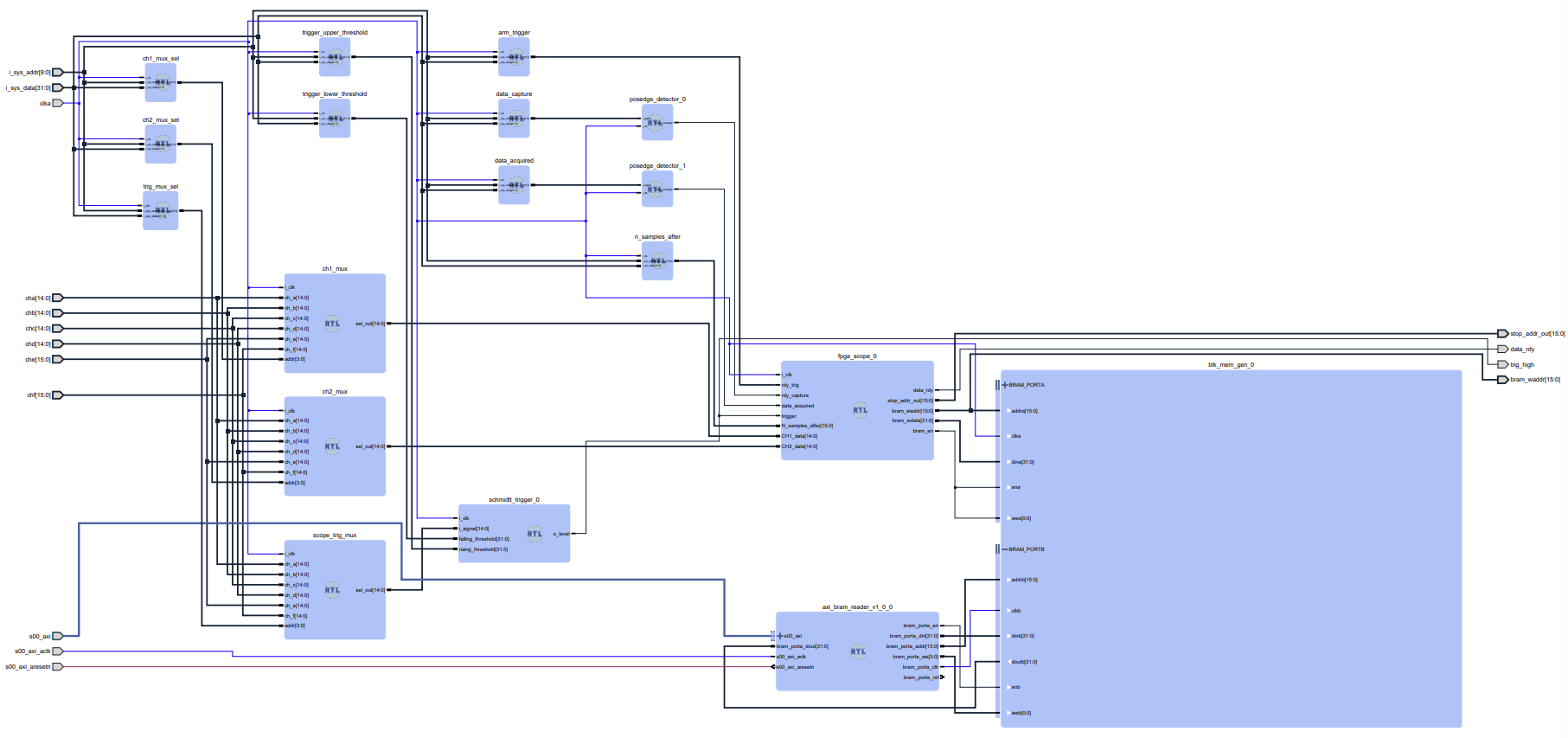
Scope:
Here’s the FPGA scope, which uses a dual-port BRAM to write trace data from the FPGA fpga_scope.v, and is read by an axi_bram_reader for the CPU-side to access from.
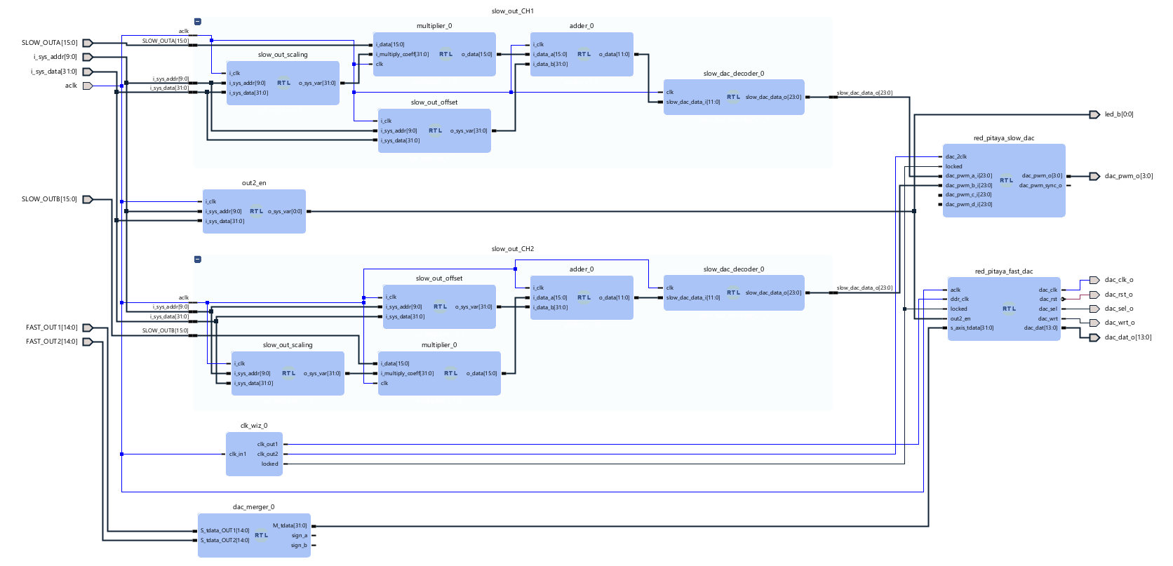
Analog IO:
Here’s the output scaling bit-manipulating blocks used to output to the slow PWM DAC outputs (100 KSP/s) and the fast DAC outputs (125 MSP/s):
FIR:
And here’s a small FIR filter example I made, which you can find more about in the FIR development post under 3. FIR and CIC Filters.
.png)
2. Server-Client Networking
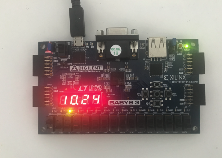
In previous FPGA projects, I’ve used a Basys-3 FPGA, which uses Xilinx Artix-7. This is nice, but because it’s only an FPGA, interacting with the system needs to be done with physical buttons and switches, and reading data from it comes just from LED or seven segment displays:
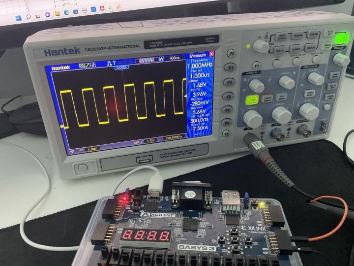
However, for a large platform this gets out of scale really quickly. The Red Pitaya board we use in this project has a Zynq-7010, which has both an FPGA and an ARM Cortex A9. These two are interconnected, so data can be written/read to the FPGA from the CPU side.
On the A9 is a python server file waiting for incoming update commands, which is unpacked into a set of binary data which is written to physical memory that is shared with the FPGA. The FPGA accesses this data at a specific memory address, and writes it to its local data registers.
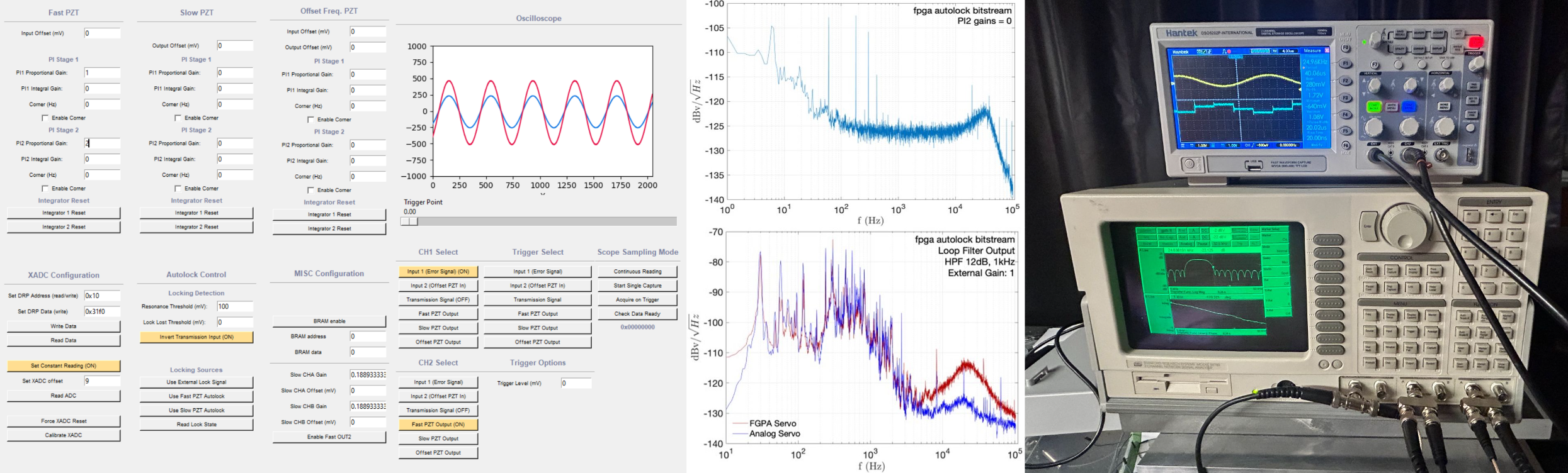
To connect to this server, I also wrote a python client file that has a GUI for users to modify system parameters. The client file is a multithreaded program running a GUI thread, and a data socket thread. These two talk with each other through a set of thread-safe queues to send data packets, scope traces, and coefficients between each other. Here’s what it all looks like for the user:
.png)
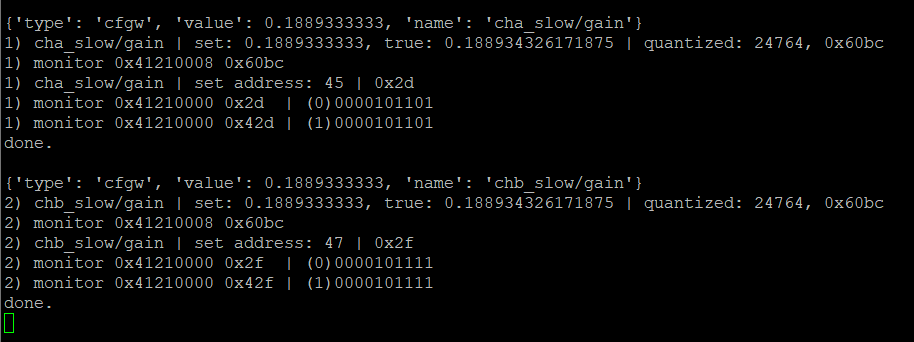
An incoming JSON packet indicates to the server the type, value, and location for a new coefficient / constant to be stored. In this case I’m trying to change the output DAC gains on channel A and channel B. Using a lookup table this gets converted into an address (0x2d, 0x2f), and the quantized data is placed into memory:
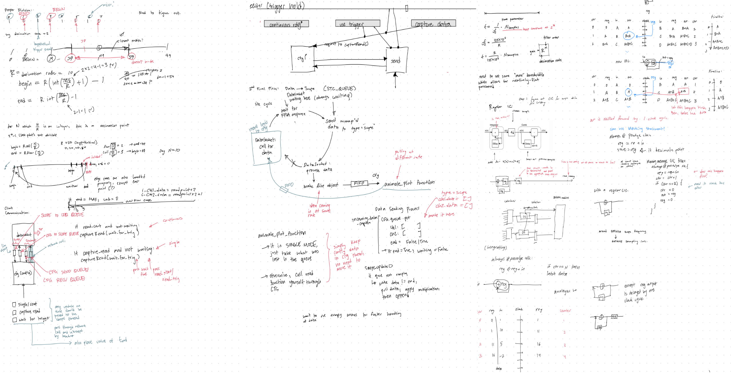
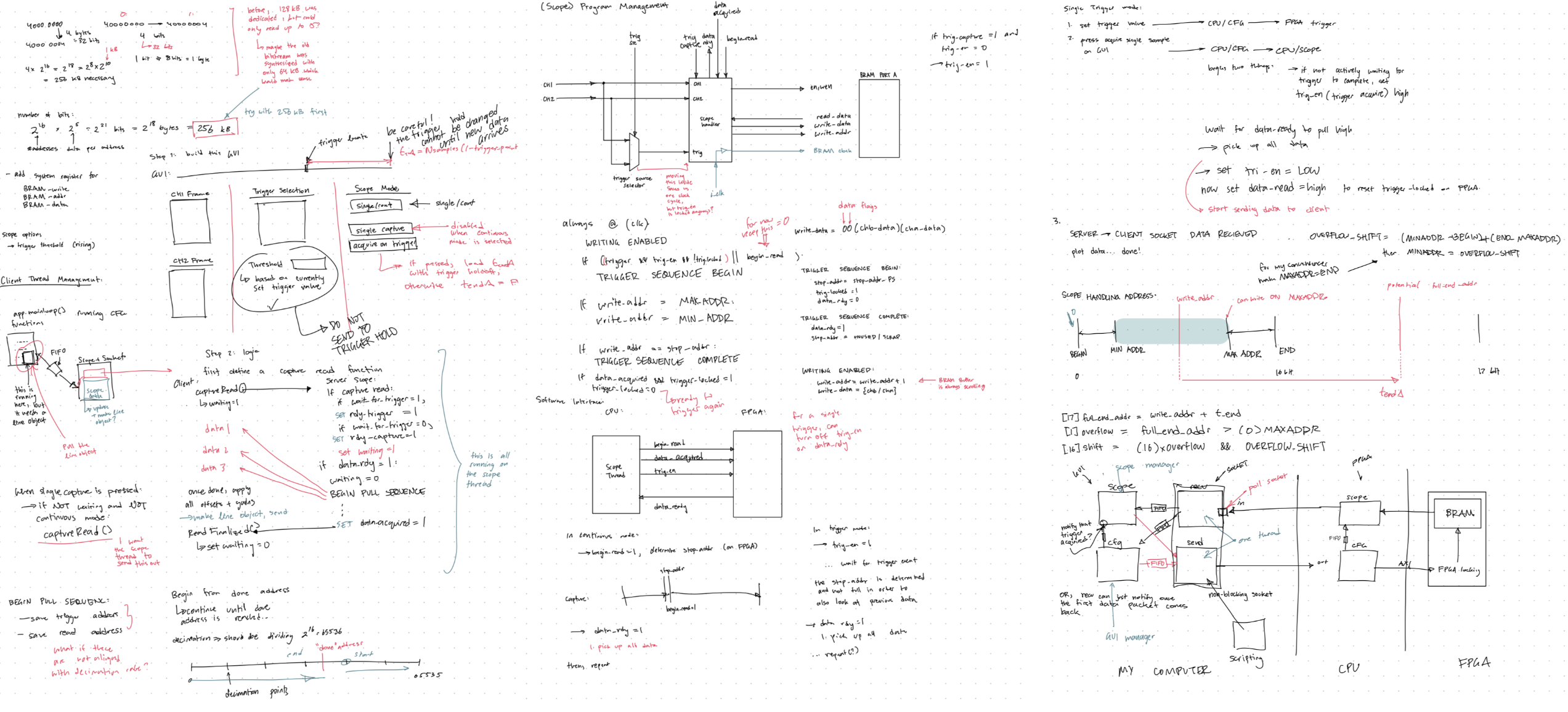
And for designing the server, client, their data sharing, and how the scope will pull data asynchronously while the user can still key in coefficients, we have notes. Lots and lots of notes.
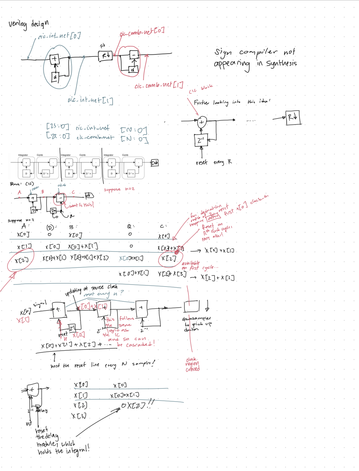
3. FIR and CIC Filters
These are more precise development posts which have extra walkthroughs:
One of our first projects before starting any laser locking was trying to get a simple runtime-adjustable FIR / CIC filter chain working.
They ended up working really nicely for our purposes — here’s an example of a bandpass filter with 31 taps, with a maximum bandwidth of ~100 kHz. The left is the theoretical response plotted by a MATLAB tool (available in FIR development post), and the right is the experimental response. They’re essentially identical!
.png)
Transfer Function (orange = 0 dB)
.png)
Transfer Function (orange = x1 gain)
.png)
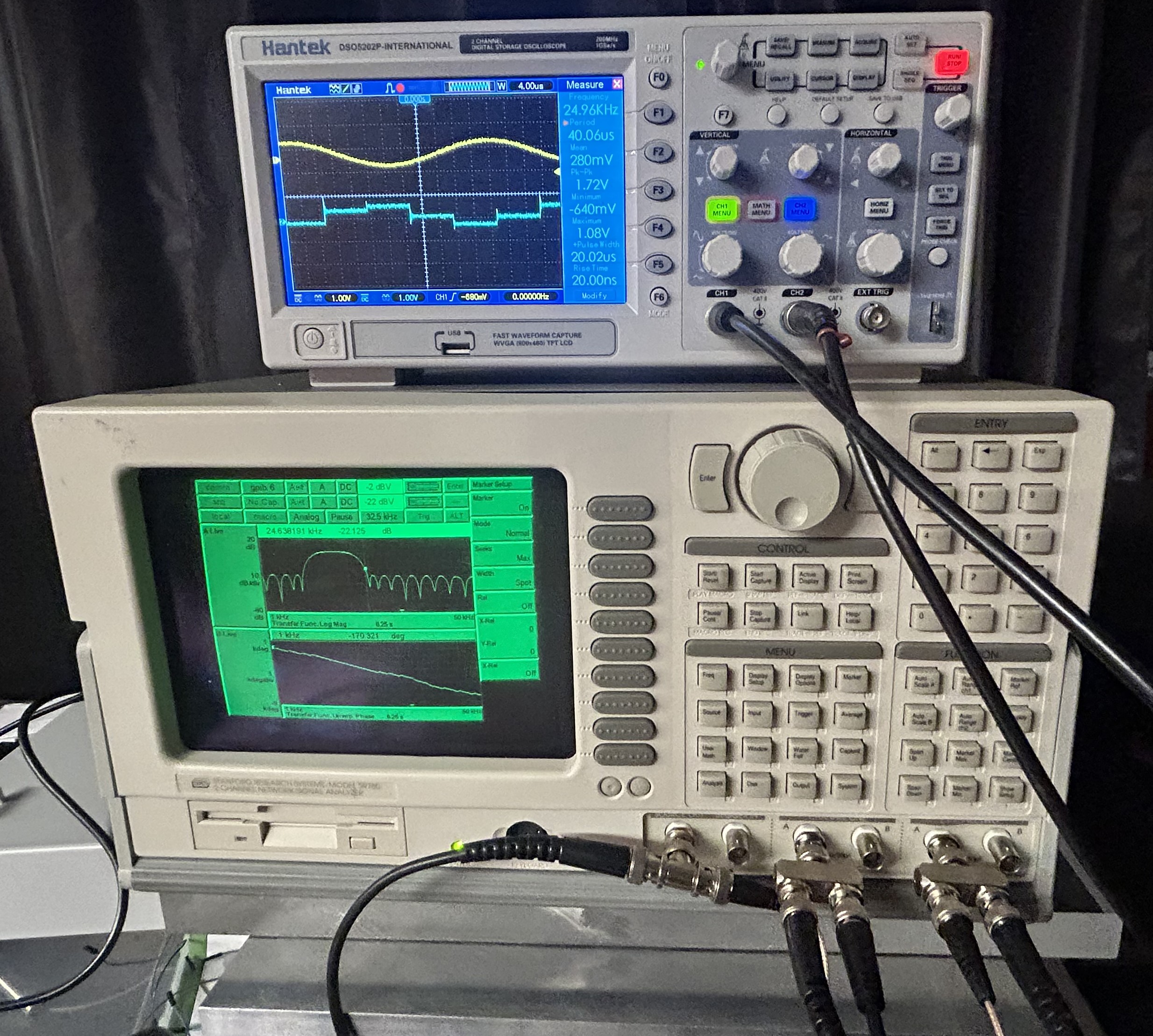
Normally we use the Analog Discovery 2 for quick and dirty testing, but for applications where we need to study crosstalk, noise floors, transfer functions, and frequency responses, we use the SR780 Signal Analyzer made by Stanford Research Systems:
Anyways, here’s how the filter and associated infrastructure are configured in the block design:
.png)
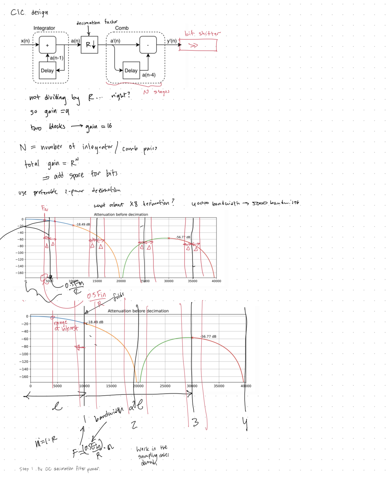
The CIC development mainly involved creating a tool to help analyze the frequency response and worst-case passbands in MATLAB:
.png)
I want to give credit to this page I used as a reference, which was a really nice visual step-through of designing and simulating a CIC down-sampler … and more notes!
4. PID Motor Control
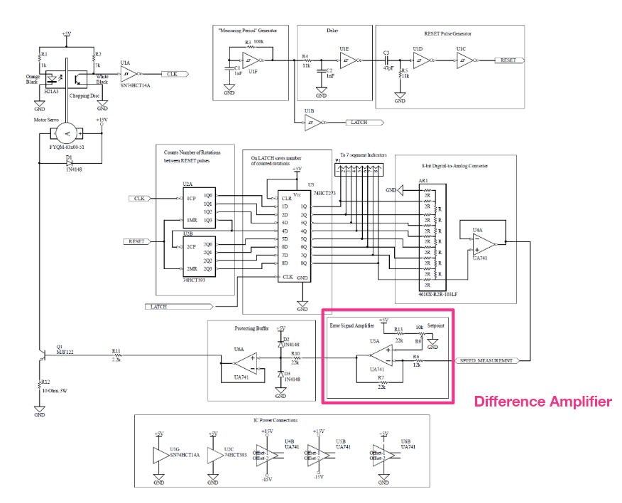
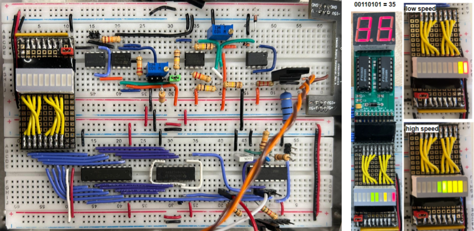
In ENPH 259, we make a closed-loop motor speed controller. In short, a motor has a rotary disk on it with 10 holes along the circumference, creating a break-beam. Every rotation, 10 pulses of light reach the phototransistor. By measuring the amount of pulses within a certain period of time we measure some factor of speed (rotations / period). This is converted to an analog value and then passed into a difference amplifier — the output of this is then fed back to the motor, creating a closed loop.
Here’s the circuit built and powered (motor not shown), and the LED bar indicates the speed.
To get more acquainted with the FPGA and it’s DSP and analog IO capabilities, one “mini project” we set out to complete was to replace the difference amplifier with an FPGA PID controller. I put together the proportional and integrator blocks:
.png)
The error and setpoint values come into the FPGA, and the output of the controller goes to the current-controlling transistor. From the top its hooked up like this:
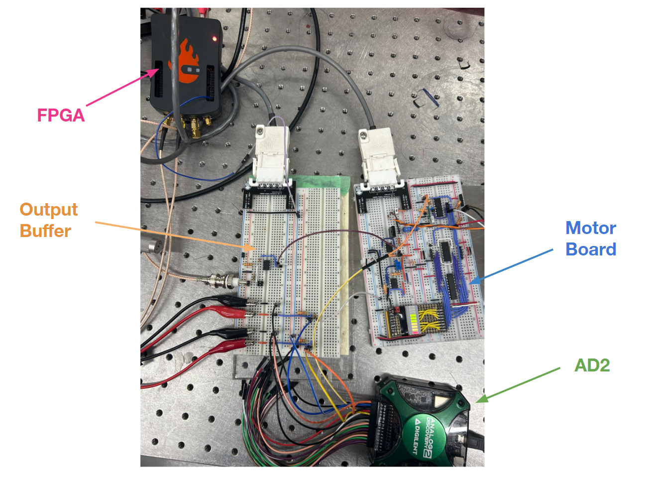
The motor board still does the speed measurement, but now that analog signal is passed into one of the FPGA inputs — this is the process variable. The AD2 is outputs a DC setpoint variable which passes into the second FPGA input.
The error = process - setpoint is passed into the FPGA PID and then comes out on an analog output. This is buffered using the output buffer and this signal is given back to the motor board’s current-controlling transistor.
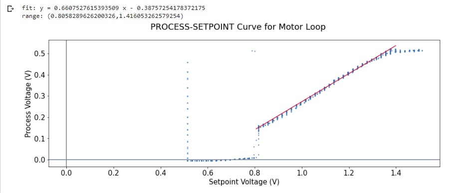
If we try just using P gain on the FPGA, we see that the process voltage (speed we’re driving the motor at) never reaches the setpoint voltage (voltage corresponding to the speed to drive at). In other words the P control isn’t doing enough to eliminate the steady state error.
Here’s another representation, with the setpoint being the orange trace and the blue trace is the process variable.
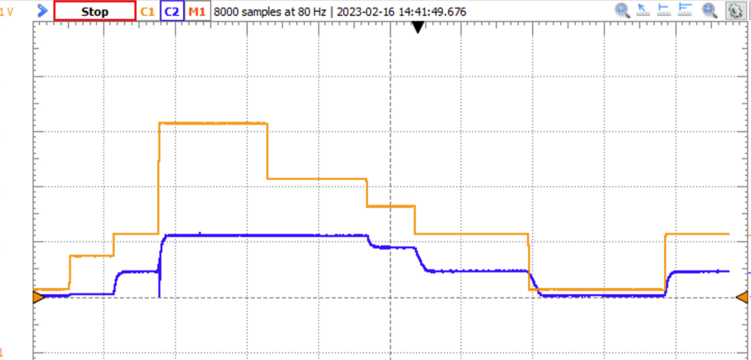
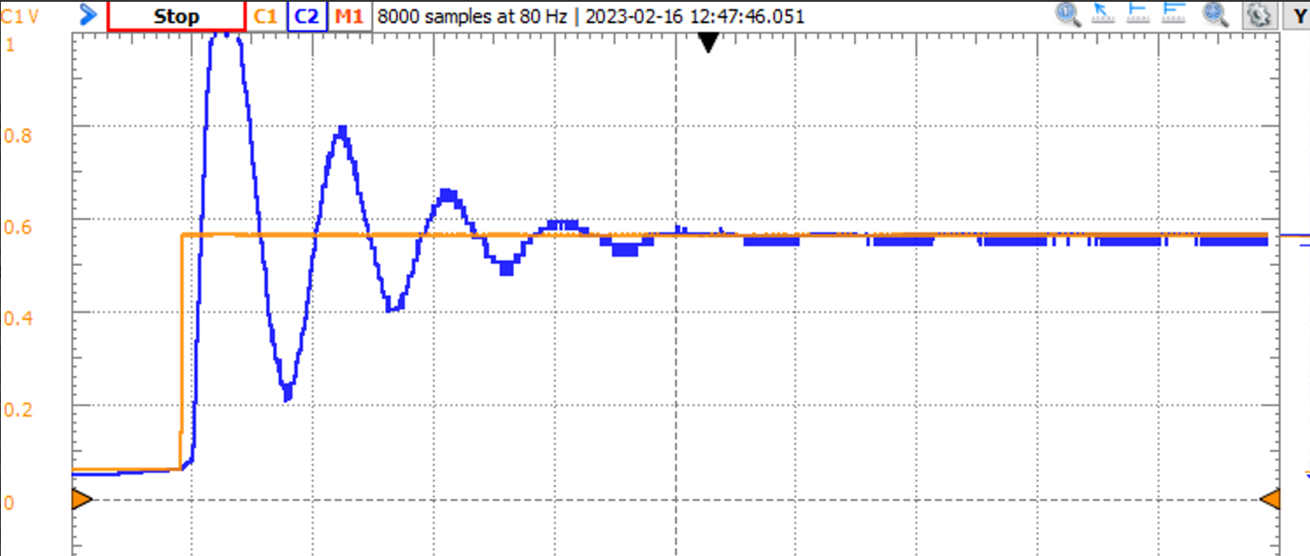
But now, if we add some integrator gain, we get curves like this, with the average steady state error being driven to 2mV!
.png)
Here’s another curve showing the step response of the PID controller — of course, this is completely untuned, but it’s somewhat satisfying seeing these curves which you see in textbooks all the time come to life in a real control loop.
Overall, this short mini tangent in our exploration of FPGAs and using a PID to control a motor’s speed was successful, and it was from here where we started diving more into the real laser cavity work to follow.